
The 10-Second Story: Virtual Twins and ML Revolutionize DRAM Yield Optimization
In the relentless pursuit of semiconductor advancement, achieving optimal DRAM yield has become a critical bottleneck. Traditional methods struggle with the escalating complexity of manufacturing processes, where systemic failures often derail progress. This report details a groundbreaking approach leveraging calibrated virtual twins and advanced machine learning (ML) to dramatically enhance DRAM yield optimization, pushing success rates from a mere 0.1% to an impressive 78.5%.
Table of Contents
Unlocking Manufacturing Efficiency with Virtual Twins and AI
As memory technologies shrink and processes become more intricate, the challenge of maintaining high manufacturing yields intensifies. The introduction of additional process steps, tighter control windows, and novel sources of variation create a complex landscape for engineers. Systemic failures, driven by intricate interactions across multiple process modules, are emerging as a significant cause of yield loss during the critical ramp-up phase.
The Bottleneck of Systemic Failures
Rapidly identifying the root causes of these systemic defects is paramount for accelerating time-to-market and improving yield. However, conventional failure analysis, heavily reliant on time-consuming and costly wafer experimentation, is proving insufficient. This is precisely where the integration of virtual manufacturing models, or ‘virtual twins,’ combined with ML-driven optimization offers a transformative solution.
Process engineers can now utilize sophisticated virtual manufacturing models, such as SEMulator3D, coupled with ML optimization tools like Fabtex Yield Optimizer. This powerful combination allows for the prediction of process failures and the evaluation of potential yield improvements with significantly reduced reliance on physical wafer experimentation. This approach promises to accelerate the learning curve and shorten the path to targeted manufacturing yields.
Architecture and Implementation: Building the Virtual DRAM Twin
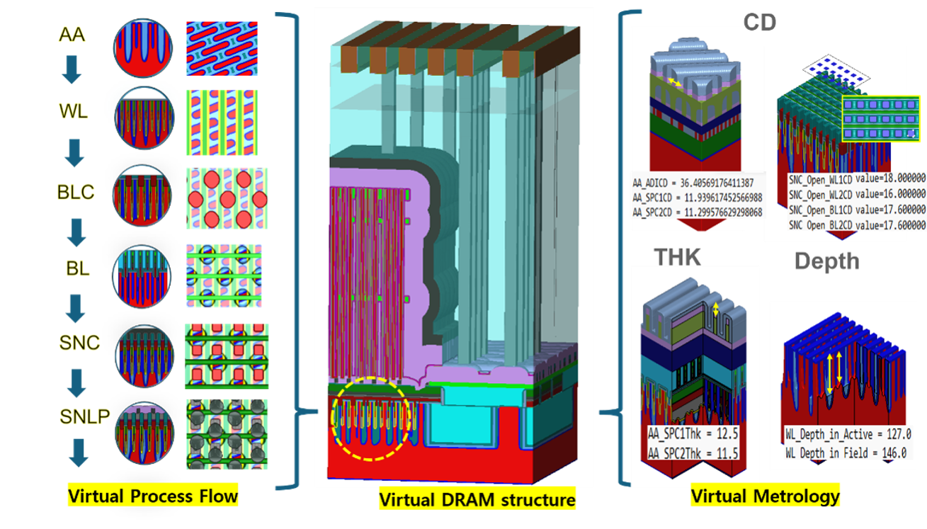
The core of this advanced methodology lies in constructing and calibrating a precise virtual twin of the DRAM manufacturing process. This virtual environment meticulously replicates the physical fabrication steps, incorporating virtual metrology measurements at critical junctures throughout the sequence. This allows for real-time monitoring and data collection within the simulation, mirroring the in-fab metrology crucial for process control.
Calibrating the Virtual Environment
Once the virtual twin is established, machine learning algorithms are employed to calibrate the model against actual silicon data. This calibration process ensures that the virtual environment accurately reflects observed manufacturing behaviors, providing a robust foundation for subsequent failure analysis and optimization tasks. For a specific case study, a calibrated virtual twin was developed for a DRAM memory device, incorporating eight known systemic failure mechanisms.
These failure modes, including shorts, opens, and overlap-related defects between critical DRAM structures, were meticulously modeled. By defining virtual metrology to detect each specific failure mode—translating geometric conditions into measurable parameters—engineers could automatically detect and analyze multiple failure mechanisms concurrently within a single simulation study. This simultaneous analysis is a significant leap from traditional, sequential failure analysis methods.
Engineering Trade-offs and ML-Driven Optimization
With the calibrated virtual twin in place, ML algorithms were unleashed to dissect the impact of process and structural variations on the eight predefined failure modes. The objective was to identify an optimized manufacturing solution—specific process adjustments—that would minimize the failure rate across all identified modes. Unlike conventional approaches that tackle failures in isolation, the ML optimization routine evaluated the collective impact of multiple process changes simultaneously.
Simultaneous Failure Reduction
The optimization process actively searched for process targets that collectively improved the overall pass ratio. As demonstrated in the study, the optimized process settings led to a substantial reduction in all eight systemic failure modes. This holistic approach ensures that improvements in one area do not inadvertently exacerbate issues in another, a common pitfall in complex manufacturing environments.

Under the initial nominal process conditions, the predicted total yield stood at a mere 0.1%. Post-optimization, this figure dramatically surged to 78.5%, reflecting significantly lower failure rates across all eight failure mechanisms. This dramatic improvement underscores the power of ML in navigating complex, multi-variable optimization problems inherent in advanced semiconductor manufacturing.
Field Readiness and Future Verdict
The insights gained from this virtual analysis are not confined to simulation; they translate directly into actionable inline fab targets. Engineers receive precise guidance on which process and structural parameters require adjustment to further mitigate systemic failures in the real production environment. This bridges the gap between simulation and physical implementation, accelerating the yield ramp and improving overall manufacturing efficiency.
Accelerating Innovation in Chip Design
This work powerfully demonstrates how the synergy between detailed process models and sophisticated ML can accelerate yield improvement during DRAM device development. By accurately replicating process variability in a calibrated virtual environment and performing simultaneous optimization, engineers can efficiently detect multiple device failures and explore a vast solution space without the prohibitive time and cost associated with extensive silicon experimentation. This methodology is akin to how advanced simulation and AI are being explored in other complex fields, such as optimizing AI chip design itself, as seen with initiatives like Oxmiq Unlocks AI Chip Design for India. The future of semiconductor manufacturing hinges on such intelligent, data-driven approaches.
The ability to rapidly iterate and optimize designs in a virtual space, informed by real-world data, is crucial for staying competitive. This methodology not only speeds up the development cycle for DRAM but also sets a precedent for tackling yield challenges in future generations of memory and logic devices. The successful application of these techniques promises to lower costs, improve device performance, and accelerate the delivery of next-generation semiconductor technologies to the market.
Source: Semiconductor Engineering